 With most modern PC based digitizers and data acquisition systems a common problem is caused by the fact that the ADC technology usually runs in advance of PC bus technology. In high-speed and high-resolution digitizer products this causes a bottleneck effect where the ADC can digitize much more data than can be easily transferred to the PC environment. For example, USB based digitizers commonly boast acquisition sampling rates higher than 100 Mega-samples per second (MS/s) but data transfer speeds to the PC are often limited by the bus to only a few MBytes/s. This bottleneck effect leads to situations where the digitizer has to stop acquiring data, potentially missing important events, while it waits to clear previously stored information. Furthermore, the slow transfer rates limit a systems overall measurement and analysis speed. This becomes a major concern in applications where large amounts of data have to be collected, stored and analyzed.
Approaches to the bottleneck problem
One approach to solving the bottleneck problem is to send the data to on-board Field Programmable Gate Arrays (FPGA's) where the end user can process the data and endeavor to reduce the amount of information that needs to be sent over the bus to the PC. However, at high speeds, this approach is usually quite expensive as it requires costly FPGA firmware development tools and specialized engineering knowledge. Developing advanced FPGA firmware is not a simple task and, depending on the algorithms being implemented, can take an extensive amount of time before the firmware is designed, debugged and operational. This sort of investment only makes sense for very large projects.
Spectrum has taken another approach to try and make it much easier for the digitizer user. The solution combines the latest in PC bus technologies with factory engineered FPGA routines and a number of smart data acquisition and transfer modes. The result lets the user easily optimize the data transfer process and allows complex measurement and analysis routines to be performed within the PC environment. Once there, off-the-shelf software tools such as MATLAB from MathWorks, NI's LabVIEW or Spectrums own SBench 6 can be used to process the in-coming data. This approach eliminates the need for customized firmware thereby simplifying project developments and greatly reducing engineering costs.
| Bus Type | Typical sustained data transfer rates |
|---|---|
| USB 2.0 | ~35 MB/s |
| GBit Ethernet/LXI | ~70 MB/s |
| PCI/PXI/cPCI | ~100 MB/s |
| PCI-X 66 MHz | ~240 MB/s |
| PCIe/PXIe x1 lane Gen1 | ~170 MB/s |
| PXIe x4 Gen 1 | ~700 MB/s |
| AXIe (PCIe based backplane) | ~1.5 GB/s |
| PCIe x8 lane Gen2 | ~3.4 GB/s |
| PCIe x16 lane Gen3 | ~12.8 GB/s |
Table 1 shows a number of digitizer interfaces and the typical data transfer speeds that they can sustain for extended acquisition periods. From the table it is easy to see that digitizers built on the slower or older bus systems such as USB or PCI can easily encounter data transfer bottlenecks if the on-board ADC's are digitizing at moderate speeds in the 10-200 MS/s range or higher. The problem is further compounded if the digitizer has multiple channels as this effectively multiplies the amount of data that's being acquired.
PCIe, a truly high-speed bus
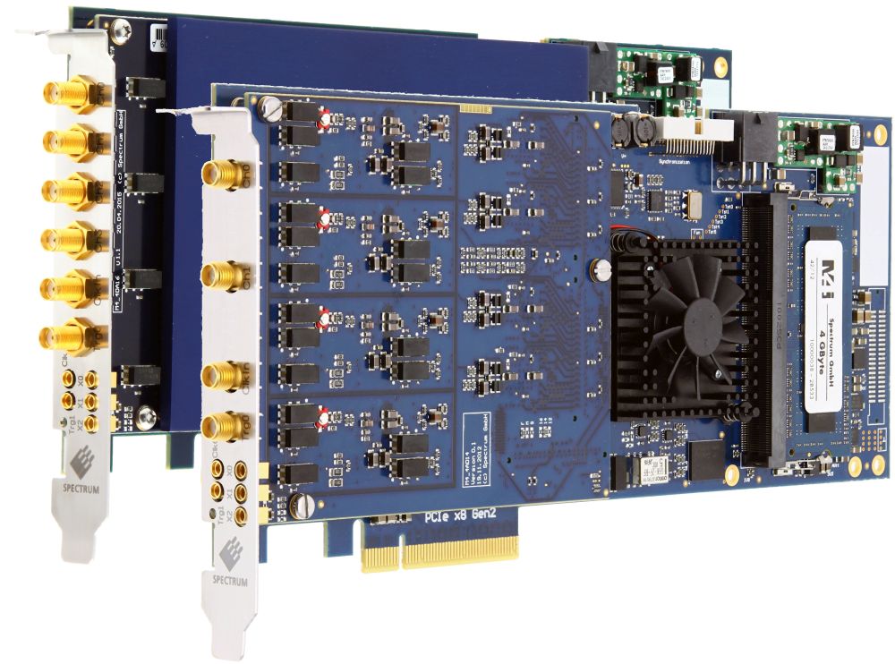
Of course the data transfer speed doesn't simply depend upon the bus of the digitizer. It will also be influenced by other factors such as the PC, its setup, and the software being used to control the transfer process. Figure 1 shows Spectrum's M4i.22xx and M4i.44xx series digitizers which offer sampling rates as high as 5 GS/s with 8 bit resolution, 500 MS/s with 14 bit resolution, or 250 MS/s with 16 bit resolution. These M4i series cards all feature the latest in PC bus technology for digitizers, a PCIe x8 lane Gen2 interface, that's capable of transferring data from the on-board memory to a PC at rates up to 3.4 GB/s. The M4i series cards come with speed optimized drivers for Windows and LINUX and multiple busmaster DMA (direct memory access) engines are used to help maintain the fastest possible throughput rates.
How to measure the DMA data transfer speed
The DMA transfer performance is result of all the different components that are involved. The Digitizer manufacturer has influence on the Digitizer FPGA DMA core, the kernel driver, the library and the test program. The PC motherboard also affects the overall performance. On one hand there are hardware factors such as the number of connected PCIe lanes, the supported PCIe generation and the number of bridges between the CPU and the slot. On the other hand there are software elements like the BIOS, BIOS settings and the payload size which may depend on other components used in the system.
To measure the DMA performance for this article we have used the Spectrum Control Center, a small software tool for Spectrum products that allows maintenance and testing. The Spectrum Control Center is a C++ application based on the Qt libraries that allow it to run on both for Windows and Linux operating systems. To measure the DMA transfer speed the card is switched into a special speed test mode to avoid any influence of the particular card model. For example, a 2 channel 500 MS/s 14 bit card can only generate 1953 MB/s of data when running at full sampling speed - that's not even near to the performance that an 8 lane Gen2 PCIe bus can actually transfer.
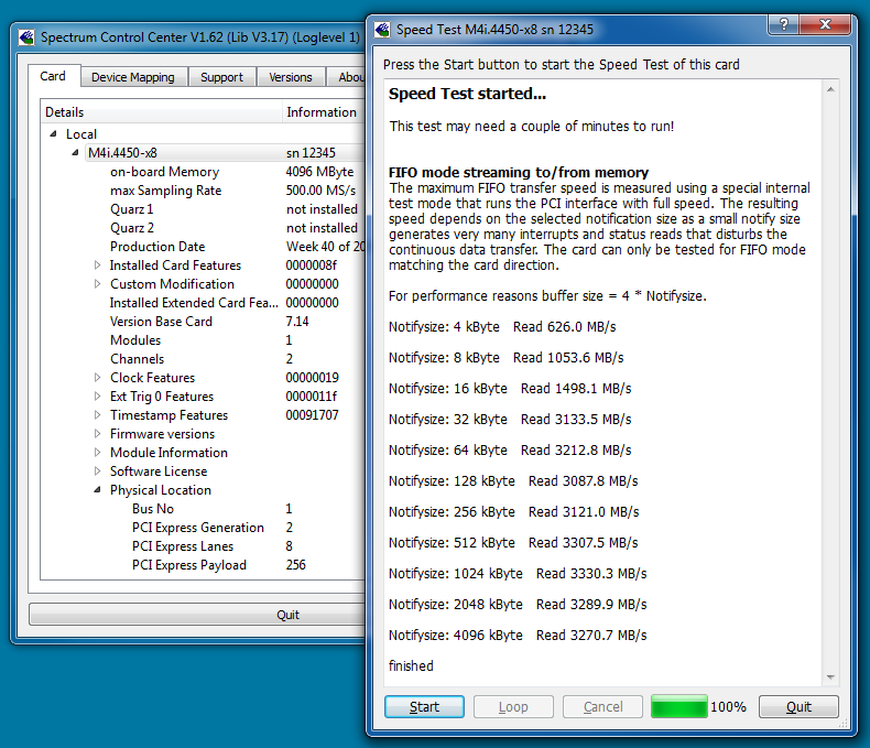 Since PC motherboards and their BIOS structure differ the results also depend on the DMA notify size - that is the amount of data that is transferred after which an interrupt is issued. For maximum performance the optimal notify size needs to be selected for the DMA transfer. The Spectrum Control Center iterates different notify sizes to find the best performance settings. This is shown in figure 2. In this example good performance is reached when a notify size of 32 kBytes or above is used. The maximum transfer speed is at 1 MByte notify size, which when used means handling an interrupt every 300 us. For the motherboard used in this test the maximum DMA transfer performance is 3330 MB/s. The information screen of the Control Center also reveals that the PCIe payload size for the slot used is 256 bytes, which leads to the best transfer performance.
The command line tool shown in figure 3 is also available as source code to customers. With this tool users can easily adjust the DMA settings and test data streaming with real world settings to hard disk arrays.
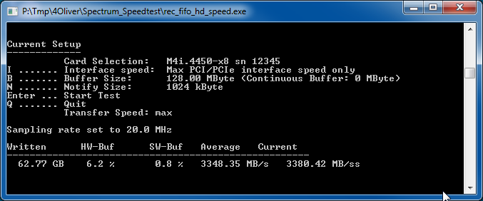 As seen in figure 3, the performance is slightly better (an average of 3348 MB/s) as there's no graphical user interface involved. This tool can also be used to measure the DMA performance of multiple cards in parallel motherboards, where it will reveal their bottlenecks in terms of insufficient PCIe lane connections.
The effects of different motherboards and payload settings
Table 2 shows some benchmark testing results where an M4i series digitizer was used with different PC motherboards and configurations. The best performance is achieved with a PCIe payload size of 256 Bytes. The motherboard manual explains how the slots are electrically connected, as not every mechanical 8 lane slot connects all lanes to the chipset.
| Motherboard Type | Slot Connection | Payload Size | Measured Transfer Speed |
|---|---|---|---|
| Supermicro X9SLR | PCIe x8 Gen3 | 256 | 3375 MByte/s |
| Gigabyte H77-D3H | PCIe x16 Gen3 | 256 | 3360 MByte/s |
| ASRock Z97 Extreme 4 | PCIe x8 Gen3 | 128 | 3030 MByte |
| Asus Z8PE-D12X | PCIe x8 Gen2 | 256 | 3288 MByte/s |
| Supermicro X9SLR | PCIe x4 Gen3 (electrically) | 256 | 1697 MByte/s |
Smart Read-out Modes
In addition to the fast PCIe bus the M4i digitizer cards are also equipped with different acquisition modes. The standard acquisition mode uses the on-board acquisition memory as a ring buffer just like an oscilloscope. Data is written in the ring memory of the digitizer until a trigger event occurs. After the trigger, post-trigger values are recorded. This results in both pre- and post-trigger values being included in the recorded data.
The other acquisition mode is FIFO (first in-first out). This is a streaming mode which is designed for continuous data transfer between the digitizer and an external host computer. The control of the data stream is handled automatically, by the driver, based on an interrupt request.
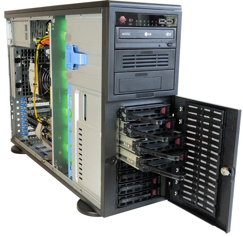
The main difference between the standard and FIFO modes is that the standard mode is limited to using on-board memory, which is 4 GByte on the M4i series. The FIFO mode is designed to transfer data continuously over the bus to PC memory or to hard disk and can therefore run for much longer acquisition times. The complete, installed acquisition memory is used as a buffer, providing reliable, data streaming. Full streaming performance needs a dedicated RAID controller, a bunch of SSD's with high throughput, an optimized driver, the correct system and software setup as well as streaming software that can get around the bottlenecks of the operating system. Spectrum offers such a turn-key solution as shown in figure 4 which allows continuous streaming of several TBytes of data to an SSD array with > 3 GByte/s transfer speeds.
Memory segmentation modes for low duty cycle measurements
 The standard and FIFO modes can also be used with three different multiple recording methods. Multiple recording can be used whenever the signal to be digitized arrives in bursts or in a sequential manner. Multiple recording allows more efficient use of the on-board acquisition memory, particularly in low duty cycle measurement applications. Low duty cycle applications include those which have short duration events of interest followed by long quiescent intervals. The acquisition methods optimized for the capture of this type of signal are Multiple Recording (segment) mode, Gated mode, and ABA (dual time base) acquisition. All of these modes segment the memory and make multiple acquisitions within it. The dual time base ABA mode reduces the sampling rate between triggers saving memory space but providing a view of what is happening in the dead-time between triggers. For further information explaining these acquisition and multiple recording modes please refer to the application note "Using modular digitizer acquisition modes".
On-Board Analysis
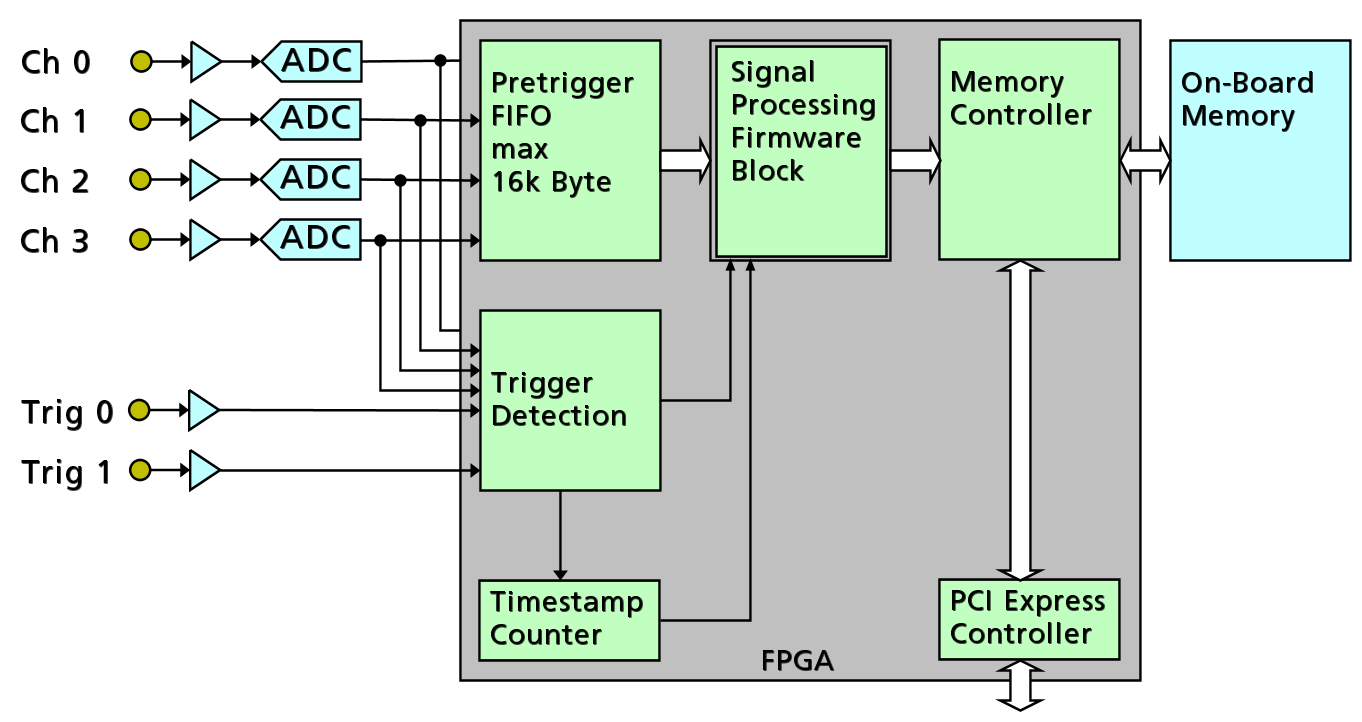 The final method one can use with the M4i series digitizers to overcome the data bottleneck problem is to use on-board processing and data reduction. The M4i series cards incorporate in their design an FPGA that is used for a variety of functions that include memory control, triggering modes, PCIe bus control and signal processing. Figure 5 shows the block diagram and basic architecture of an M4i series digitizer. Inside the FPGA space is reserved so that it can be loaded with factory developed firmware for functions such as signal averaging, peak detection and statistics.
On-board signal processing can reduce the final amount of data that needs to be transferred to the PC by orders of magnitude. For example, when working with recurring signals the Averaging firmware is capable of accumulating over 65,000 individual waveforms, each up to 128 kpoints long. The function effectively reduces the data from all the individual waveforms to one single averaged one.
Similarly, peak detection firmware can locate maximum and minimum events within a signal and store their values together with their corresponding timing information. In this way waveforms that previously contained thousands, or even millions, of data points can be reduced to a simple set of perhaps six to eight basic numbers.
Conclusion
As the ADC technology deployed in modern digitizers reaches faster acquisition rates, with higher resolution, the amount of data that needs to be acquired, stored and transferred to a PC continues to increase. Shifting the data into the PC for viewing, storage and analysis requires a digitizer design that has an appropriate bus (capable of sustaining comparable data transfer rates), flexible acquisition and transfer modes, a well configured PC and suitable software. In extreme cases, where data reduction becomes a necessity, FPGA technology can also be employed.